Matching FET’s

Vk2sja-Photo30

So the next thing on the building agenda was yet another piece of test gear. I want to start by building the Minima KISS mixer. The focus of so much attention recently as some builders were having trouble with it. And because the LO to RF port isolation was being reported as not being high enough. Having read as much as I can understand about the topic (very little but I’m learning). I’ve become convinced that success with a mixer made from two FET devices probably entails careful “matching” of the FET’s. After all, we match the diodes we use in the simple BFO mixer. So why not the FET’s?

From “Mixer Musings and the KISS Mixer by Chris Trask / N7ZWY:”

“…but that the balance of such a mixer making use of discrete transistors will be poorer than the balance of a diode mixer because of the difficulty of matching the rather complex transistor parameters over the operating range (10).” 10. HF Radio Systems & Circuits, 2nd ed. Noble Publishing Co., Atlanta, Georgie, 1998

Where the transistors mentioned above are VHF FET’s. So the problem would seem well known.

Having decided that matching FET’s is probably important, then how does one go about doing it? A quick scout around the Internet, once again led me back to the “QRP & SWL Homebuilder” website and a section called “FET Matching” (scroll down).

If by some miracle or bizarre twist of fate you are reading this and have have not already discovered “The Popcorn website”, then do yourself a favour and head on over. You’re in for a real treat.

The photo left shows my bridge variant. Setup with shorted links in the sockets where the FET’s are normally placed. This is so you can adjust the bridge balance for exactly zero volts.

Vk2sja-Photo31

So the afternoon finished with using the bridge to match some FET’s.

I was going to match a whole bunch of J310’s. Until I discovered that I didn’t have any J310’s that is! I could have sworn black and blue that I had a whole heap. Apparently not.

So I went and matched a whole bunch of Audio FET’s just for the fun of it and by way of practice. Yep, FET’s even taken from the same cardboard parts strip are all over the place!! Best match from matching 9 samples to one control was 0.010 volts. The photo opposite shows 0.313 volts but most pairings were much higher than this.

Now it should be noted that the general consensus is that for best results in a KISS mixer we should be matching the units for highest IDSS. The bridge I’ve built tells me that both FET’s are the ‘same’ but doesn’t say much about IDSS. So that’s the next experiment. Find one J310 FET with a high IDSS and then find him a partner.

Next up.. More FET matching/selection and building a KISS.

Power Supply Completed.

Vk2sja-Photo23

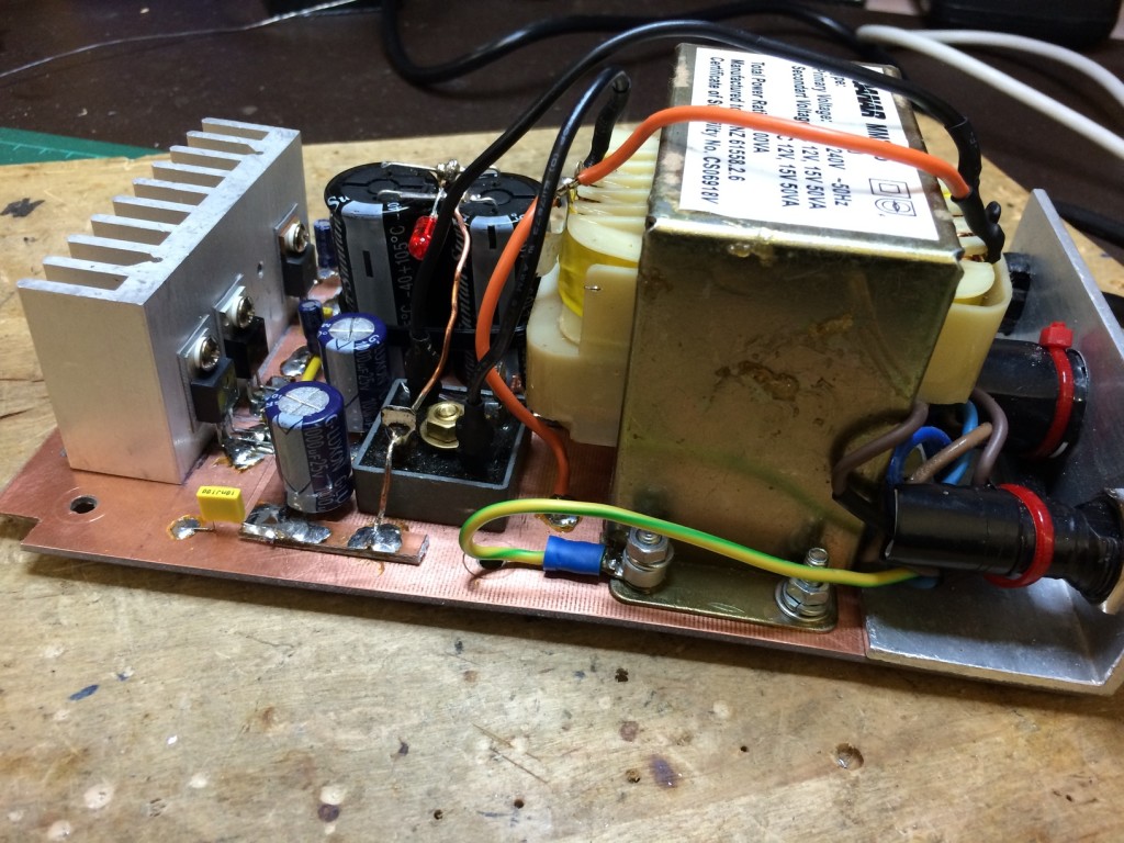
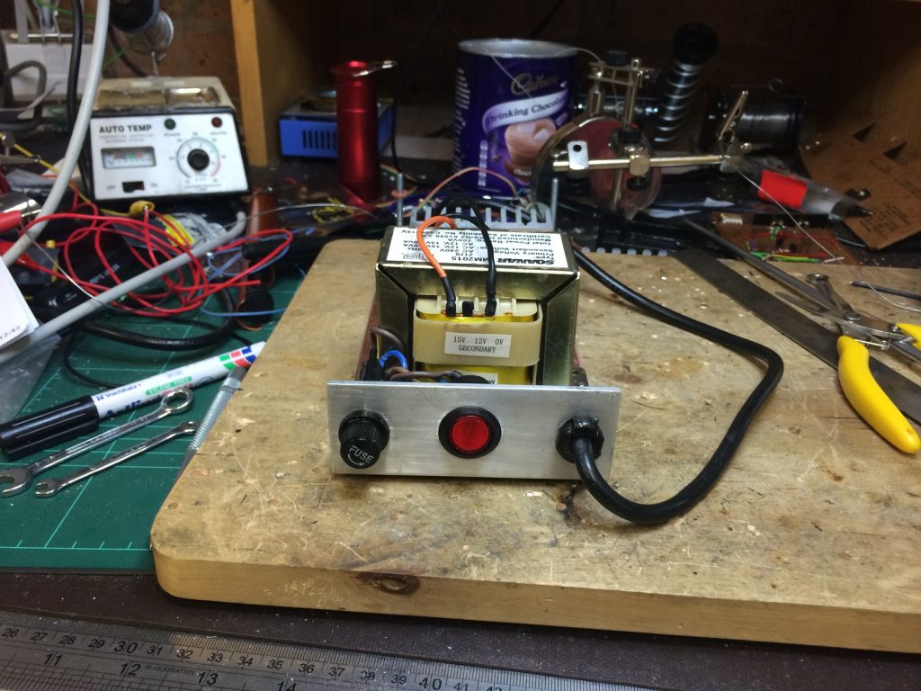
Well this is how the completed power supply turned out. For those wondering at the over-engineering. Yes, this power supply while very simple is completely over the top for a little Minima. The beauty of the Minima is that it serves as a platform for experimentation.

So I’ve build the supply with both + and -12 volt DC rails. Just in case I might want to play with split power supply audio amplifiers or similar. There is a +9v regulator that feeds from the +12 volt supply. Which in turn feeds to the +5 volt regulator on the logic board. So now the +5 regulator does not get so hot.

Vk2sja-Photo24

The supply can also provide ~40 volts DC. Which may come in handy for getting higher power from a IRF510 linear. Perhaps…

Vk2sja-Photo25

Vk2sja-Photo27

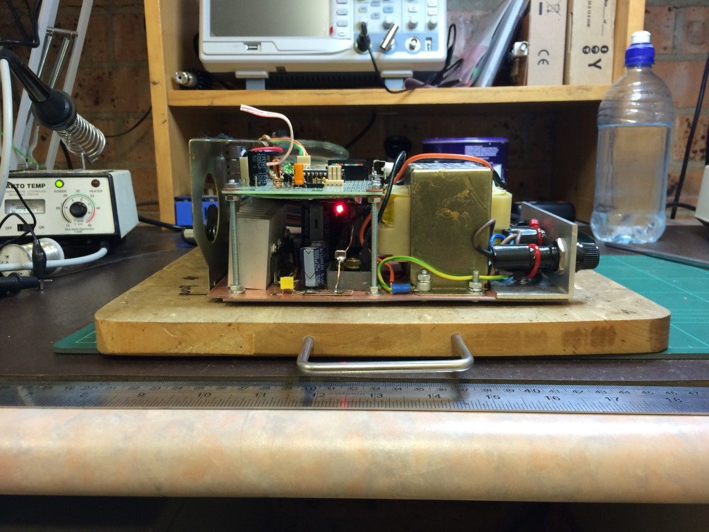
To the left is the Arduino Logic PCB mounted above the completed power supply. With the master power LED on the bleeder resistor winking out at us. “Yes I’m working and don’t poke your fingers in here!”.

To the right is the top view of the logic PCB mounted atop the power supply and the entire module bolted back onto the radio chassis.

Vk2sja-Photo28

Vk2sja-Photo29

Finally another shot of the radio powered up. This time the photo is not as contrived as previous. She is running on her own internal power supply source.

It is interesting to note that this photo was taken with the “Raduino 0.4” sign-on message displayed on the LCD screen permanently. No trick photography nor hung I2C data bus. It just happens from time to time when everything is very stable and the shack has warmed up to a nice cosy constant temperature. As soon as you move the tuning knob it starts displaying the frequency. A quick glance at the source code and I’m convinced that this is normal behaviour. The current Raduino sketch does not display the frequency until there has been some sort of update.

Mostly though when people see the “Raduino 0.4” message forever it means that the I2C data bus is in a hardware fault condition which seems to hang the Arduino Wires Library.

Work continues on the power supply.

Vk2sja-Photo20

Well another weekend of building passes. With such little time as could be devoted to the task between “life” interruptions. You will note that so eager to return to construction was I, that the work bench didn’t really get the tidy-up it urgently needed. Ah well, next time.

In the end I decided just to go ahead and complete the power supply before moving onto the radio proper. Which of course is taking much longer than expected. Here are a couple of photos of the “in progress” build of the power supply. Not yet complete but a good start. The logic board has been removed while the power supply takes shape.

Vk2sja-Photo21

I also went ahead and re-wired the ribbon cable to the logic board. So that it is now long enough to reach the new board position above the power supply. I’ve been making up ribbon cable with IDC connectors for years. And they never give me any real trouble. Until this morning that is. First attempt and no LCD display. Cable was found to have many intermittent wire faults. Any attempt to “repair” the faulty cable just seemed to make matters worse. I can normally save an IDC connector for re-use but not this time. I had to scrap the connector and start over. Second time worked a treat thank heavens. Still it wasted a good hour or two.

Vk2sja-Photo22

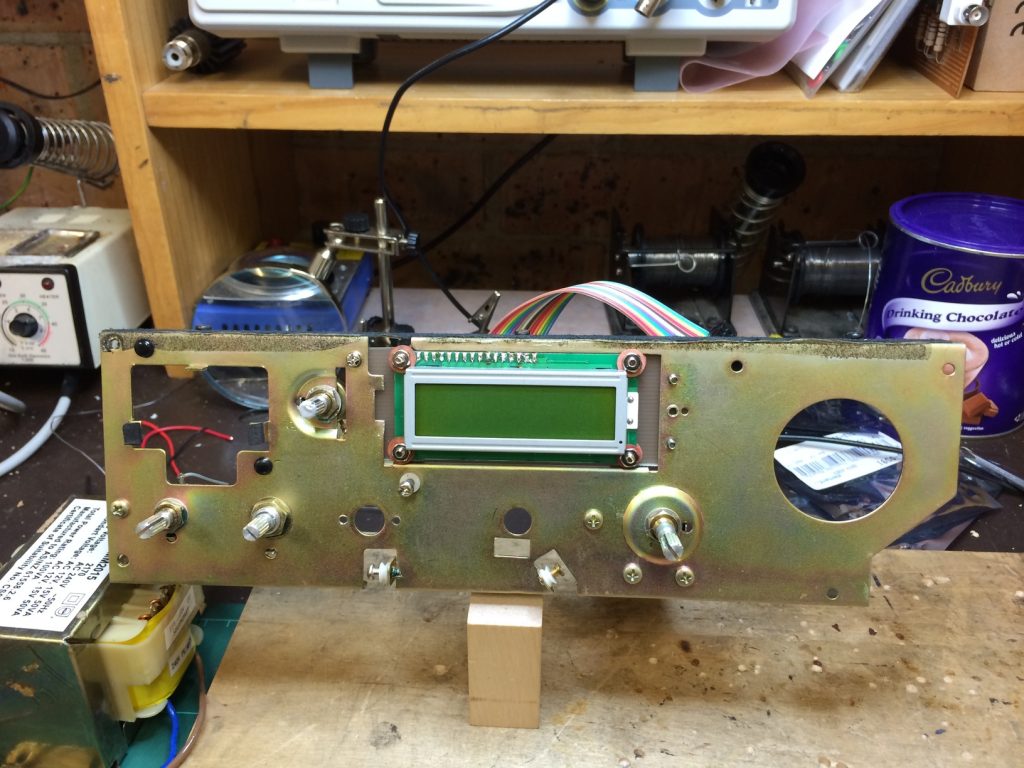
This last image is the front of the radio again. This time with the LCD powered up and displaying information under the control of the logic board. However the photo is very much contrived. As the logic board is simply dropped behind the front panel on a piece of insulating paper. Just to see what it would look like.

Next time. Hopefully the completion of the power supply. And maybe the start of the KISS mixer and some FET matching.

Mounting the LCD and preparing the case.

Vk2sja-Photo13

Well we spent the better part of a weekend preparing the case internals and mounting the LCD. All said, it turned out well enough. I am quickly learning that adapting an existing case to a new project, can in fact be just as much work as building a nice cabinet from scratch! Modern factory equipment fits together with very fine tolerances and grafting something “Alien” into said environment tends to get tricky if you’re wanting everything about the case to close back up correctly. This is a picture of the LCD mounting. This was done with small wing brackets made of PCB material. This was the second attempt, the first was with made with a set of home made aluminium brackets. Which were a failure, as the front panel could not sit flush with the case.

Vk2sja-Photo14

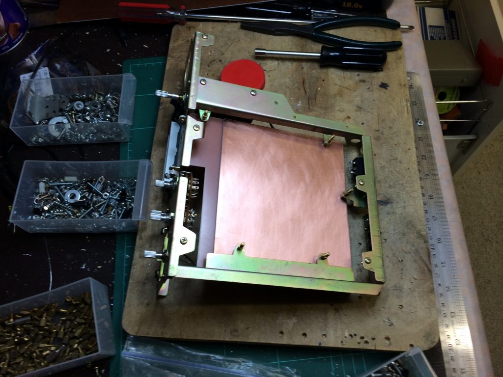
The next thing to do was add some ground plane surface area to work with. So some PCB material was cut to size. Given a spray coat of protective PCB lacquer and the result looks something like this. The rig is not a large one and I’m quite concerned about having enough raw “space” for building circuits using “Dead-Bug” or “Manhattan” style. So I wanted to be able to build circuits both top and bottom. To this end I had to use the brass PCB stand-off spacers to lift the PCB material up from where it would normally mount on the chassis. So that there would be enough room underneath for circuit components. You will note that my stand-off spacers are not fixed with bolt nuts. But instead yet more stand-off spacers are used. This is because I pulled all these brass spacers from very old PC’s many years ago and for the life of me can’t find another nut or bolt to match the thread pattern! Well, at least not in my junk-box that is. No harm done. It’s functional and I had plenty.

Vk2sja-Photo15

I didn’t have a double sided PCB board. So I simply used two sheets of single sided material back to back. Making a mental note that it is probably a very good idea to electrically join the ground-plane areas. Just so I don’t get any strange unpredictable capacitance effects. Having the top and bottom boards “separate” could make experimental life easier later on if I need to remove one or the other.

Vk2sja-Photo16

The board underneath is not cut to the exact same size and shape as the top piece simply because it was the off-cut from the top board. Waste not, want not.

Those with sharp eyes will note that an additional rotary switch has snuck into the front panel in these photos. The original band switch was connected to a shaft that activated various PCB mounted stage switches. So when the original board was removed the knob and shaft went with it. Since I plan on all the front knobs and controls being functional I needed to replace it.

Vk2sja-Photo17

Next I wanted to add another PCB and a power transformer to the otherwise unused area of the original receiver. This radio is going to be a home QTH desk job. So I’ve decided to try and incorporate the power supply into the radio. To this end a multi-tap transformer went atop another slice of PCB material. Power supply to be built later.

Then I needed somewhere to mount my radio logic Ardunio board. So this was done over the top of what will be the power supply underneath. All the mucking about broke a couple of wires of the LCD display. No matter. The ribbon cable is not long enough anyway. So that’s the next job.

Vk2sja-Photo18

If one looks closely at the photo of the logic board and PSU area. You can see a problem waiting to bite the unsuspecting constructor – Hard! The left most corner of the PSU PCB material is sitting under a plastic protrusion from the front panel. This is in fact the integral front panel headphone socket. This is bending the PCB material down and placing preasure on the front panel where none should be. Look up from that point and you can see one of the front panel self-tapping screws holding the bezel in place. The result being the front panel was miss-aligned to the case body when assembled. Worse still, it resulted in that particular bezel mount point snapping off under the lateral force. So that front panel mount point had to be Super-glued back on. And it remains to be seen how strong it will be. Gluing plastics is tricky. A small section of the PSU PCB material was trimmed away with a nibbling tool to clear the headphone socket. Now the case can be reassembled and everything aligns properly.

Vk2sja-Photo19

So the day finished looking like this. Not too bad. At least the case fits back together nicely with proper alignment. I’m probably going to need to more ventilation holes. The case by the way, is predominantly made of plastic. In this last picture the main tuning knob is held in place for the “Photo Shoot” by a blob of Blue-Tack. The tuning pot that I had available with a splined shaft to match the original knob was just not long enough in the shaft to reach. So I’ve got a couple of 100K linear pots on order with a longer spline shaft which I think will be suitable.

Next up… Fixing up the LCD ribbon cable and cleaning up the shack work bench. Now that should take a day or two!!

The Arduino logic/control board.

Vk2sja-Photo5

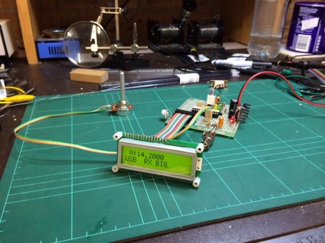
My build is going to be a “Scratch Build” with no PCB. But I decided to assemble the logic on this IC experimenters board. Which looked just about ideal for the purpose and just happened to already be in my junk box.

The Arduino ATMEGA328P IC is from an Australian company called Freetronics who make all sorts or Arduino boards and add-ons. It came with the nifty little pinout sticker on top and pre-loaded with the Arduino bootloader. So I saved myself the trouble of burning an Arduino bootloader image into a blank AVR microprocessor.

No real trouble with the build excepting for the usual debugging of ‘missing links’. Wherever Farhan’s circuit called for a 50uF electolytic I gleefully installed a 47uF instead. But apart from that it was built according to the book and worked first time.

Always very satisfying to see it “light-up” and start displaying information on the LCD.

Vk2sja-Photo10

You would think that I would be happy and leave well enough alone. But this is where I decided to modify things and got myself into trouble…

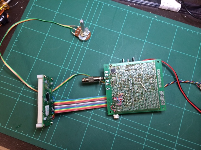
Here are two more close ups of the logic board. Both component and solder side. Never as neat on the solder side are these experimenters boards. But that’s the side you never see 😉 And it’s functional.

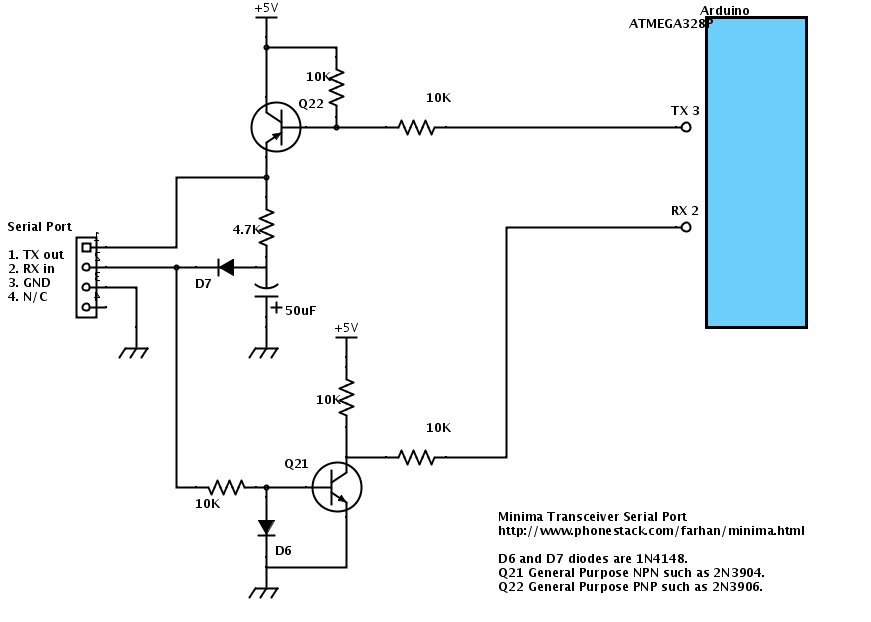
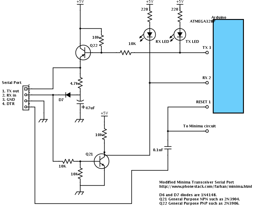
The three LED’s are Red for the +5v DC power rail. Yellow for serial data TX from the Arduino and Green for RX serial data being received into the Arduino. And this is where the trouble started. After installing the serial status LED’s it stopped working. I could no longer upload a new ‘Sketch’. I had borrowed the status LEDs from part of a circuit found on the internet here.

I played around with the resulting circuit a bit and nothing simple leapt out at me. It was starting to look like I’d have to connect the digital scope and try capture some serial data transfers so that I could see what was going wrong. Then I noticed that there was two fundamental differences in the TTL to Serial convertor from the Web Site above and the one on the Minima circuit diagram around transistor Q21. The Minima had a diode from the base of Q21 to ground were the internet circuit had a 10K resistor. The other difference was that the path between Q21’s collector and pin 2 (RX) on the Arduino was via a 10K resistor. But the internet circuit was a direct link with no resistor. So being lazy I quickly made both of these changes and “wham” the serial port started working again. Both directions and with pretty status LED’s.

Another very important modification was the addition of a 0.1uF capacitor between the Reset pin 1 of the AVR microprocessor and the serial port DTR (Data Terminal Ready) pin. Pin 4 on a DB9 connector. This enables the Arduino IDE to pulse a reset to the micro just before it starts a new sketch upload. This makes programming new firmware very easy, works every time, no manual intervention with the reset switch.

I’ve reproduced the original and modified circuits below.

Minima-Serial

Minima-Serial2

Step one, tear it apart!

Vk2sja-Photo2

So we start by tearing the old girl apart and adding the contents therein to the junk-box collection. Never throw anything out if you can help it. This was what was inside at the start of the process.

Vk2sja-Photo3

The last photo is one of the white dial marker line removed. I didn’t want to see that in front of the LCD display. Several solvents were tried to remove it. Each with cotton wool buds. What seem to be called Q-Tips in other parts of the World. Each applied carefully to the very edge of the window so that we could see the results. In the end good old “Methylated spirits” did the job of substantially removing the white line without destroying the Perspex window.

More coming soon. Next up, my Minima logic board.

My Minima build finally starts

Vk2sja-Photo1

Well I’ve been dragging the chain a bit. Delaying the start of my Minima build until I could get some of my other projects squared away. But finally I have started.

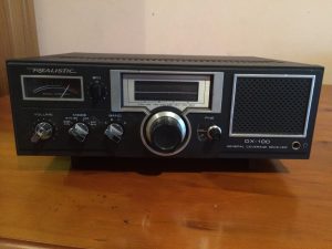
Now I just know that this will probably upset someone who started their Radio career many years ago by listening to a Realistic DX-100 HF receiver. So I’ll say sorry up front. Sorry.

But I’ve had this Realistic DX-100 kicking around for some time. It is a *very* basic HF receiver. I picked it up at a second hand store and it had a fault on one band that I could never be bothered to try and fix. Good looking radio, terrible receiver! Time passed and I came across the BitX design and I thought that this radio would make an excellent donor case for a BitX project. As it had both a large tuning knob and a fine tune control. I was just about to start building a BitX when Farhan released the design of the Minima.

I looked at the Realistic DX-100 with new ‘eyes’ and that dial window looked just about perfect for a LCD display. And it is!

So now with a quick change of direction this old receiver is destined to become a Minima!

Radio Projects for the Amateur


20131030-093145.jpg

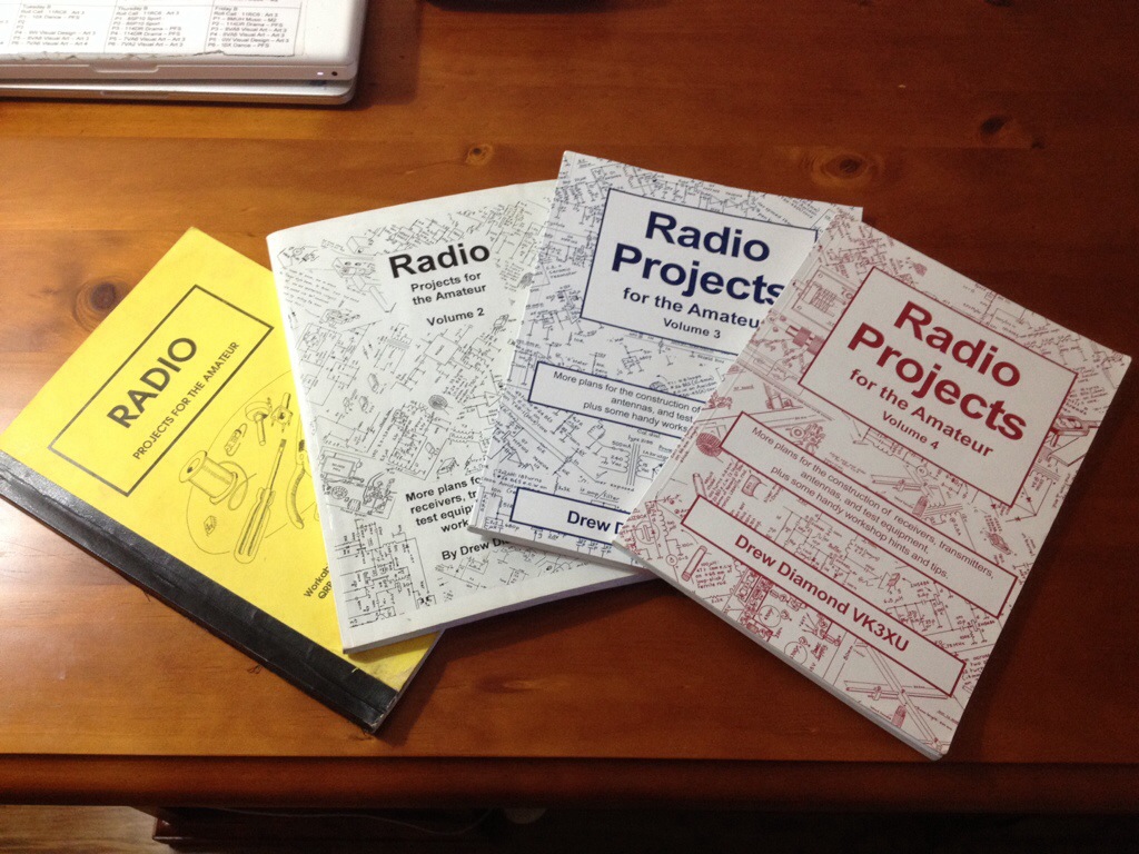
I guess before I move on to “blogging” about some of my own home-brew radio projects I’d best do another quick book review. Well four books in fact. And the reason for doing this up-front is because many of my personal shack projects come from one of these publications.

I’m talking about “Radio Projects for the Amateur” available in no less than four volumes. All created by Drew Diamond VK3XU. To say Drew is prolific in publishing first class radio construction articles is probably something of an understatement.

Much of the content (but by no means all) contained in these books originally appeared in “Amateur Radio” magazine. The journal of the Wireless Institue of Australia (WIA).

For a long time certain volumes were out of print and unobtainable unless you got lucky on the second hand market. At the time of writing all volumes appear to be available from the Wireless Institute of Australia (WIA) Bookshop. I would happily encourage anyone interested in home-brewing to grab all four while they are still available. 100% pure gold!

ozQRP MST400

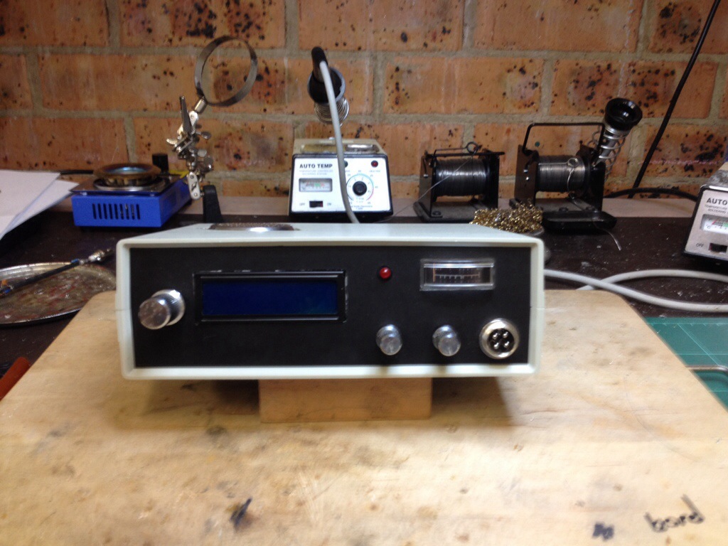
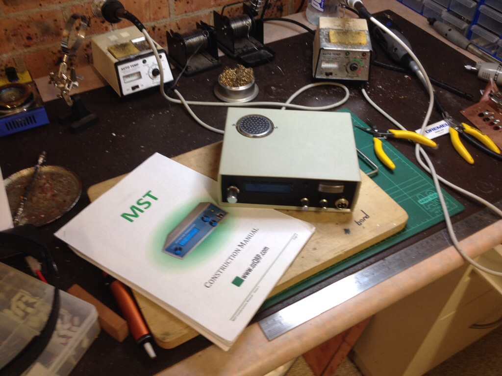
Here are some (very poor quality) photos of the current project. An ozQRP, MST400 the MST standing for “Minimalist Sideband Transceiver”. Available as a partial kit in two versions, 40m and 80m. I’m building the 40m version designated MST400. The kit comes with the PCB and optionally some hard to find parts. You source the rest of the parts yourself. The parts sourcing issue elevates this kit to an intermediate level of difficulty. This is not a beginners kit.

20131029-104607.jpg

Front view. Plastic box (finding good, cheap metal boxes is so hard – sigh). Metal front and rear plates. Silver knobs from a very old defunct crystal CB radio (Yeah, I know, never use metal knobs!). The fact that the two smaller knobs don’t line up properly shows up in the photo! It’s not so noticeable when your holding the radio. I’ll have to do something about that. The misalignment is due to the way I mounted the pots (more on that in a minute). The signal strength meter is from the same discarded CB radio.

20131029-104623.jpg

Top view. Speaker grill is a sink drain filter. Not sure if I like the look or not. But it’s functional. Next time I might just use it as a template and drill holes in the plastic. The construction manual is alongside. The manual is absolutely excellent! Not quite the Elecraft “step-by-step” gold standard but very good for the intended audience.

20131029-104636.jpg

I had a roll of aluminium foil (flashing) with adhesive backing. Available from hardware stores and used for insulation. I used it to insulate the box from RF. I mounted the DDS VFO, a separate but matching kit (you can supply your own VFO if you prefer) and the controls to a PCB set rearwards from the front panel. Rather than mounting them directly to the front panel. This makes it easier to keep the front panel looking neat and builds a RF shield between the DDS VFO and the main transceiver PCB. Probably not required but it seemed like a good idea.

20131029-104653.jpg

Another shot of the case top cover. Showing speaker, sink drain speaker grill and aluminium insulation.

20131029-104710.jpg

Front panel and DDS control board. Upside down. Not only can I not take in-focus pictures I get them upside down as well! I’ll fix it later.

20131029-104727.jpg

Here is the cause of the pot alignment problem. Because of the pot shaft length that I had on hand I decided to try and solder the pot body directly to the PCB. It works. But the precise alignment is quite difficult without building an alignment jig to hold the pots in place while soldering. And if you build that jig, out of say PCB material, then you may as well make it permanent! Ah, well, live and learn.

Copper foil construction

Some time back I read about an Amateur who had discovered a copper foil with an adhesive backing. He was experimenting with using it for PCB
construction. At the time I thought;- “I must try that”. It took quite some time but I finally found some to play with.

20131029-094044.jpg

Now I wish I could properly credit where the original idea came from (It was not mine) but it was so long ago I’ve forgotten which Journal I was reading. Perhaps GQRP Sprat or maybe even VK-QRP Lo-Key.

Anyway, I finally found some copper foil. The like of which I think was being referred to in the original article. I found it on eBay (where else) and ordered a small roll. I gather it’s intended purpose is for creating RF shielding for enclosures.

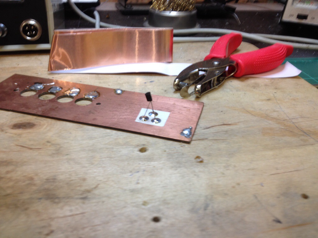
The blurred image above (Sorry, I’ll take some better photo’s later) shows the result. A paper hole punch for creating confetti dots was used to punch out some pads. Three dots were then stuck to a white sticky label on top of the PCB. Then a transistor was soldered to the dots.

So “Yes”, it works.

Is it quick and easy? So much so that I won’t be picking up my Dremel again? No, not yet. At least not without some refinement. The cheap hole punch causes the foil to buckle. A more expensive two-hole punch works fine but you can’t easily see to properly align the holes your punching. So you end up with a lot of wastage. Of course it is dead easy to cut odd-shaped rectangles with a pair of scissors.

Even the act of removing the backing tape from the “dot” and sticking it down is fiddly and somewhat time consuming.

I also worry about the stray capacitance between the copper foil sticker and the copper sheet of the PCB proper. The two being separated only by the width of a paper sicker. Stray capacitance could get quite high here.

But with some refinement the technique shows obvious promise. So while the Dremel may not be due for retirement any time soon I can see a “hybrid’ construction technique developing.

Utopia would be a box of 500 easily dispensed white paper dots, each containing three little copper dots.

Anyway, I’ll keep playing with the idea.